1 Test Purpose
The purpose of this examination is to nondestructively detect unbonded regions and voids in the die attach material of semiconductor devices through the measure of acoustic continuity. It establishes methods and criteria for ultrasonic inspection of semiconductor devices.
The ultrasonic generator, receiver, and line scan recorder settings (when used) shall be selected or adjusted as necessary to obtain satisfactory images and achieve maximum image details within the sensitivity requirements for the device or defect features the test is directed toward. In the case of reflection mode or transmission mode images, care must be exercised to insure that the ultrasound penetrates and is sensitive to the entire die attach interface.
2 Test Objectives and Principle
Plastic Package and semiconductor Component
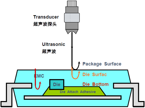

Fig. 1: Test Principle
3 Typical Case Study
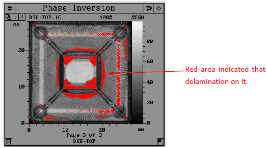
Fig. 2: Case Study
4 Test Effect
(1) Batch Quality Uniformity Inspection
(2) Key Process Quality Monitoring
(3) Delivery Component Inspection and Sampling
(4) Out of Storage Re-inspection and Sampling
(5) Daily Inspection or Application Inspection
(6) Identifying and re-New component Assessment
(7) Components Reliability Screening and Qualification
(8) Quality Analysis and Comparison
(9) Control the related process failure mode during Design and Production

公众号

Add.(Office):16th Floor, Building AB, Southern Securities Building, No. 2016 and 2018 Jianshe Road, Jiabei Community, Nanhu Street, Luohu District, Shenzhen City, Guangdong Province
Tel.: +86-769-22247299 E_mail: Service@itstlab.com
Add.(Laboratory):1F, no.278, wentang shiyang street, dongcheng district, dongguan, guangdong.
Tel.: +86-769-22247299 E_mail: Service@itstlab.com
Add.: 407, 3 building, No. 3, Science Avenue,Guangzhou Science Park,Guangzhou City,P.R.China.
Tel.: +86-20-29862950 E_mail: Service@itstlab.com