PCB/PCBA Failure Analysis
1 Purpose
In order to ensure and improve the quality and reliability of electronic products, the failure analysis must be performed on failed samples, to find the root cause of product failure, and through the implementation of targeted improvement.
2 Key Failure Mode (But no limited)
Poor soldering Bending deformation Corrosion or migration
Determination / Blister Open Circuit Short Circuit
3 Failure Analysis Technology Method
Appearance Inspection Thermal analysis SIMS
X-Section C-SAM FT-IR
X-Ray FIB Failure Simulation Analysis
Dry & Pry SEM & EDS TEM
4 Benefits
- Identify the reason of the failure, provide the evidence for product design, material optimization and process improvement;
- Clearly the responsible of failure reason, and provide the evidence for judicial arbitration.
5 Case Study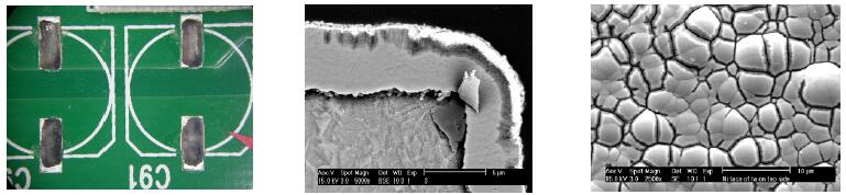
PCB Poor Soldering (chemical nickel)

公众号

Add.(Office):16th Floor, Building AB, Southern Securities Building, No. 2016 and 2018 Jianshe Road, Jiabei Community, Nanhu Street, Luohu District, Shenzhen City, Guangdong Province
Tel.: +86-769-22247299 E_mail: Service@itstlab.com
Add.(Laboratory):1F, no.278, wentang shiyang street, dongcheng district, dongguan, guangdong.
Tel.: +86-769-22247299 E_mail: Service@itstlab.com
Add.: 407, 3 building, No. 3, Science Avenue,Guangzhou Science Park,Guangzhou City,P.R.China.
Tel.: +86-20-29862950 E_mail: Service@itstlab.com