1 SEM (Scanning Electron Microscope) Analysis
SEM is a type of electron microscope that produces images of a sample by scanning the surface with a focused beam of electrons. The electrons interact with atoms in the sample, producing various signals that contain information about the sample's surface topography and composition. The electron beam is scanned in a raster scan pattern, and the beam's position is combined with the detected signal to produce an image. SEM can achieve resolution better than 1 nanometer. Specimens can be observed in high vacuum in conventional SEM, or in low vacuum or wet conditions in variable pressure or environmental SEM, and at a wide range of cryogenic or elevated temperatures with specialized instruments.
The most common SEM mode is detection of secondary electrons emitted by atoms excited by the electron beam. The number of secondary electrons that can be detected depends, among other things, on specimen topography. By scanning the sample and collecting the secondary electrons that are emitted using a special detector, an image displaying the topography of the surface is created.
2 Key Analysis Items
- Tin
Whisker Analysis
- Element Qualitative and Quantify Analysis
- Multi-layer film thickness Measurement
- Surface or Intersecting Surface Structure Inspection and Analysis
3 Case Study
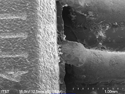

Fig. 1: IC Lead Inspection Photo (50X)
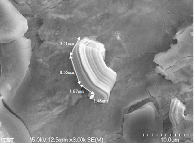

Fig. 1: IC Lead Inspection Photo (3000X) for whisker measurement

公众号

Add.(Office):16th Floor, Building AB, Southern Securities Building, No. 2016 and 2018 Jianshe Road, Jiabei Community, Nanhu Street, Luohu District, Shenzhen City, Guangdong Province
Tel.: +86-769-22247299 E_mail: Service@itstlab.com
Add.(Laboratory):1F, no.278, wentang shiyang street, dongcheng district, dongguan, guangdong.
Tel.: +86-769-22247299 E_mail: Service@itstlab.com
Add.: 407, 3 building, No. 3, Science Avenue,Guangzhou Science Park,Guangzhou City,P.R.China.
Tel.: +86-20-29862950 E_mail: Service@itstlab.com